Not all that long after that (about 18 hours ago as of this writing) a new image popped up over at VRZone that appears to change things. In the first image (shown below) you can see that there are only 11 memory chips visible (as depicted by whoever did the photoshoping there) and looking at the solder joints for the power connectors it would seem that there are 2x 8-pin connectors. This started the speculation that the card could potentially draw well over 350 Watts of power. 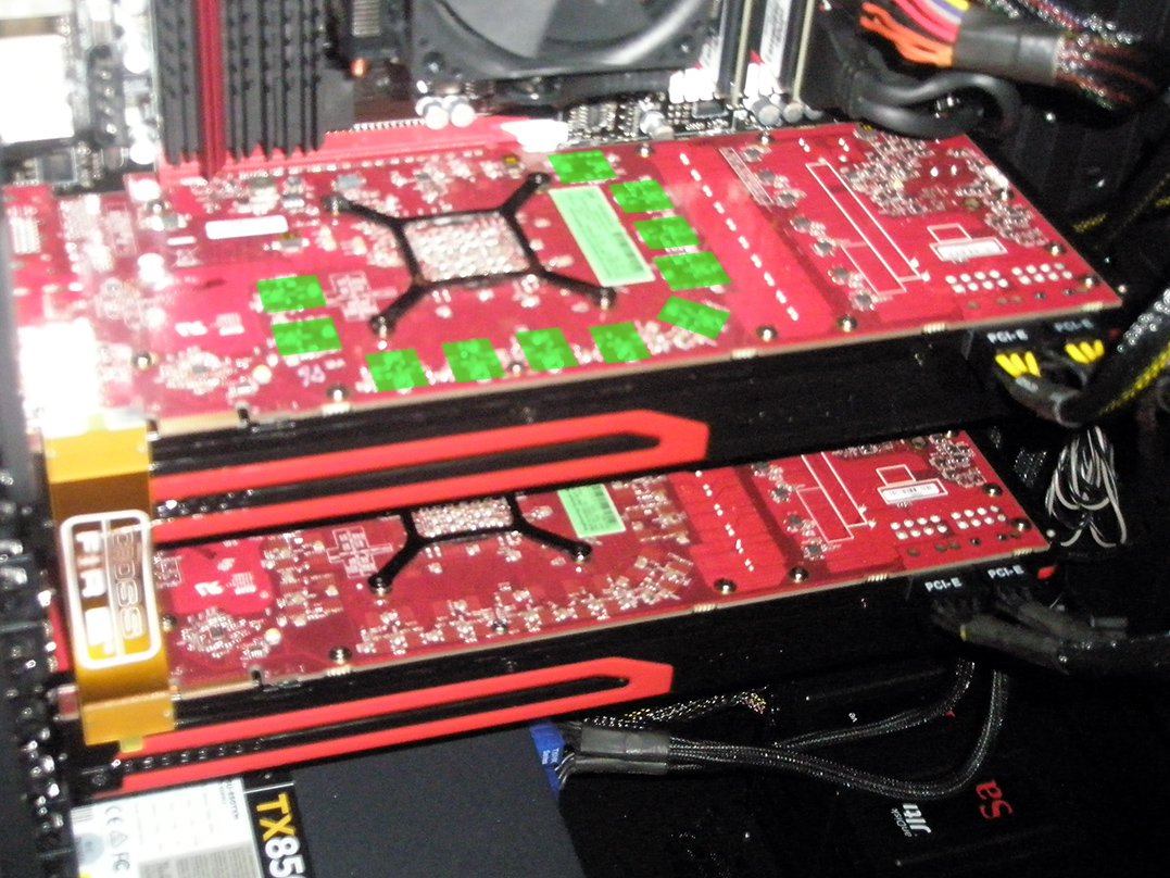
In the new images we can see a pair of 6-pin connectors which significantly reduces the anticipated power draw down from 375 Watts to around 225 (two 6-pin connectors at 75 Watts and 75 Watts from the slot). This second number is much closer to the stated specs from AMD which were around 190 Watts. The extra room is for overclocking most likely as that is something AMD started factoring in with the 5000 Series cards. Unless AMD is getting away from tradition the boards and other components will likely be built around either a 300 or 400Watt max power draw with an anticipated draw much lower. This is most likely why the early ES samples are showing up with the dual 8-pin configurations as there are sure to be some that were setup to make sure the cards could handle it.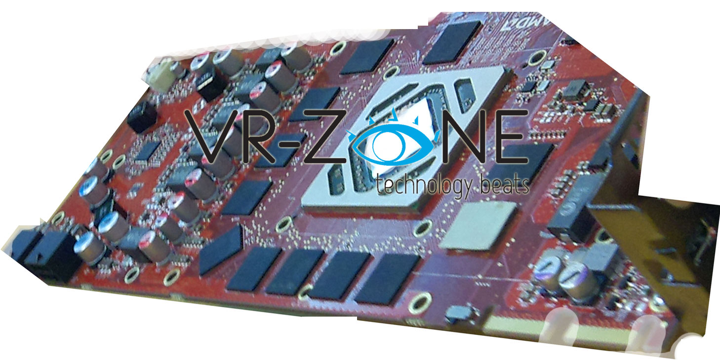
On the memory side of things it does appear to be confirmed that AMD will be pushing for a 384-bit memory interface. The rest of the specifications are anyone’s guess at this point although we are pretty sure that a new “leak” will pop up that will have those numbers sometime before the rumored January launch date.
The biggest question will be how well will these new GPUs work with AMD’s shift from their VLIW (Very Long Instruction Word) architecture to the new Graphics Core Next. With Graphics Core Next they are moving to SIMD (Single Instruction Multiple Data). This is AMD’s attempt to make a GPU that is good for both graphics AND Compute functions. We have talking in the past about AMD’s decision to use an Architecture that required a game or an application to be compiled in a certain way for good performance. This was the issue with VLIW; if your app was not compiled to properly make use of this architecture, your performance suffered. With the Graphics Core Next and its SIMD (which has also been called MIMD with an SIMD array) AMD hopes to remove this barrier and open up performance on both graphics and compute. We will get into more of the specifics of the new architecture in another article.
For now we all have to wait for the next leak to feed our curiosity on AMD’s next GPU. We will also have to wait and see how AMD’s new direction will impact these products moving forward.
Image Credits VR-Zone and Beyond3D Forum
Discuss in our Forum
Reading time is around minutes.
 Well now, it looks like there are two leaked pictures on the Internet that are reportedly of AMD’s new Tahiti GPU. The first was leaked onto the Beyond3D Forums. The image there appeared to show two of the next generation GPUs running in Crossfire. The image was enhanced to indicate where the memory chips were on the board and showed a total of 12 chips (again using small squares as indicators). These pictures much rampant speculation about what the memory architecture is as well as debate about the power requirements of this new GPU.

Latest from Sean Kalinich
- ConnectWise Slash and Grab Flaw Once Again Shows the Value of Input Validation We talk to Huntress About its Impact
- Social Manipulation as a Service – When the Bots on Twitter get their Check marks
- To Release or not to Release a PoC or OST That is the Question
- There was an Important Lesson Learned in the LockBit Takedown and it was Not About Threat Groups
- NetSPI’s Offensive Security Offering Leverages Subject Matter Experts to Enhance Pen Testing
Leave a comment
Make sure you enter all the required information, indicated by an asterisk (*). HTML code is not allowed.