Ever since the introduction of the microprocessor we have been looking for a way to make it smaller, cheaper and faster and there has been tremendous success in this over the years. If you consider the fact that CPUs were manufactured on a 250nm process back in 1998 and we are now moving to a 22nm with Intel’s next generation CPUs you can see that we have reduced the size over 10 times since 1998. The problem is that with smaller process size there is a greater chance for current leakage at the gates that control the transistors in the CPU. Both AMD and Intel have come up with different solutions for this over the years, but each one has its own size limit. Hi K Metal Gate was the last one from Intel and it did a great job down to the current process of 32nm, but now the move to 22nm is proving to be difficult. Because of this and to control leakage at this smaller size Intel is looking into a 3D lithograph in the hopes of adding more life to the current materials used for CPU manufacturing.
Something has to change in order to continue the push for smaller, faster and of course cheaper. Over the years there have been multiple materials suggested from single molecule thin sheets of Graphine to the use of carbon nanotubes (and combinations of these materials). So far none of them appear to be great leaps forward (despite being about 5 years from real use) because they also have a limit to their effectiveness. True they will extend the life cycle, but they are only buying time.
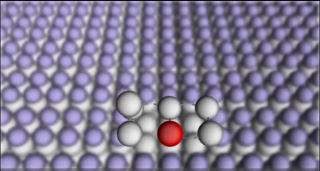
However, a research team in Australia (working off of research done about two years ago) has managed to build a transistor that is a single atom in size. This is a true breakthrough in computing and not just because they have a single atom size transistor (that was done two years ago). The real accomplishment here is that they were able to place this on a silicon crystal with precision. So far the single atom transistors created have not been precise in their placement the margin of error can be up to 10nm (or about half the size of the next process from Intel). This type of gap can introduce massive errors especially if you are pushing for something like Quantum computing (which is the goal anyway). The precision reached by the UNSW (University of New South Wales) puts the precision down to the atomic level (meaning they can place it with the precision of a single atom.
Without this type of precision there would be no possibility for manufacturing this type of transistor on a large scale which would be required for a true quantum computer to be manufactured. Of course there are still other hurdles to overcome before we can move to that level, but this is also an intermediary step in the life cycle of “common” computing devices. According to More’s Law the number of transistors in a circuit doubles every 18-24 months. This means that we would have to hit the atomic level by 2020 or so which is now only 8 years away. Considering Gaphine and Carbon Nanotubes are roughly 5-10 years from being usable to build transistors with, this type of technology is sure to be a welcome step.
Discuss this in our Forum
Who is famous for Spam worshiping Vikings? Type the Answer into the search window to go to your next clue!
News
Researchers find a way to place a single atom transitor with atomic level precision
- Details
- By Sean Kalinich
- Hits: 3464
 If you are a fan of the Douglas Adams book, the Hitchhiker’s Guide to the Galaxy (and others in the five book trilogy) then you are familiar with the great super computer Deep Though and the computer that it built to provide the question to The Ultimate Answer of Life the Universe and Everything. This was a gigantic computer that was so big it was often mistaken for a planet. It also incorporated organic life in it design (If I have lost you here don’t worry I promise I am getting to the point soon). Now in the real world researchers have found a way to use naturally occurring atomic particles to form the basis for microprocessors.


