The Layout -
The layout of any motherboard is important. Even simple mistakes in component placement or the signal traces can cause major issued in performance and stability. With the ATX form factor we find that this is even truer; the devices we drop onto them demand more and cleaner power while the signal speeds push faster and faster. Ok let’s take a look at what MSI is doing with the Big Bang Marshal. We will start with the basics; the board is an XL ATX sized (13.5-inches x 10.4 Inches) motherboard. This means that this board requires careful consideration when picking out a case. It also means that MSI has extra room for components and, as you can see, peripheral slots.
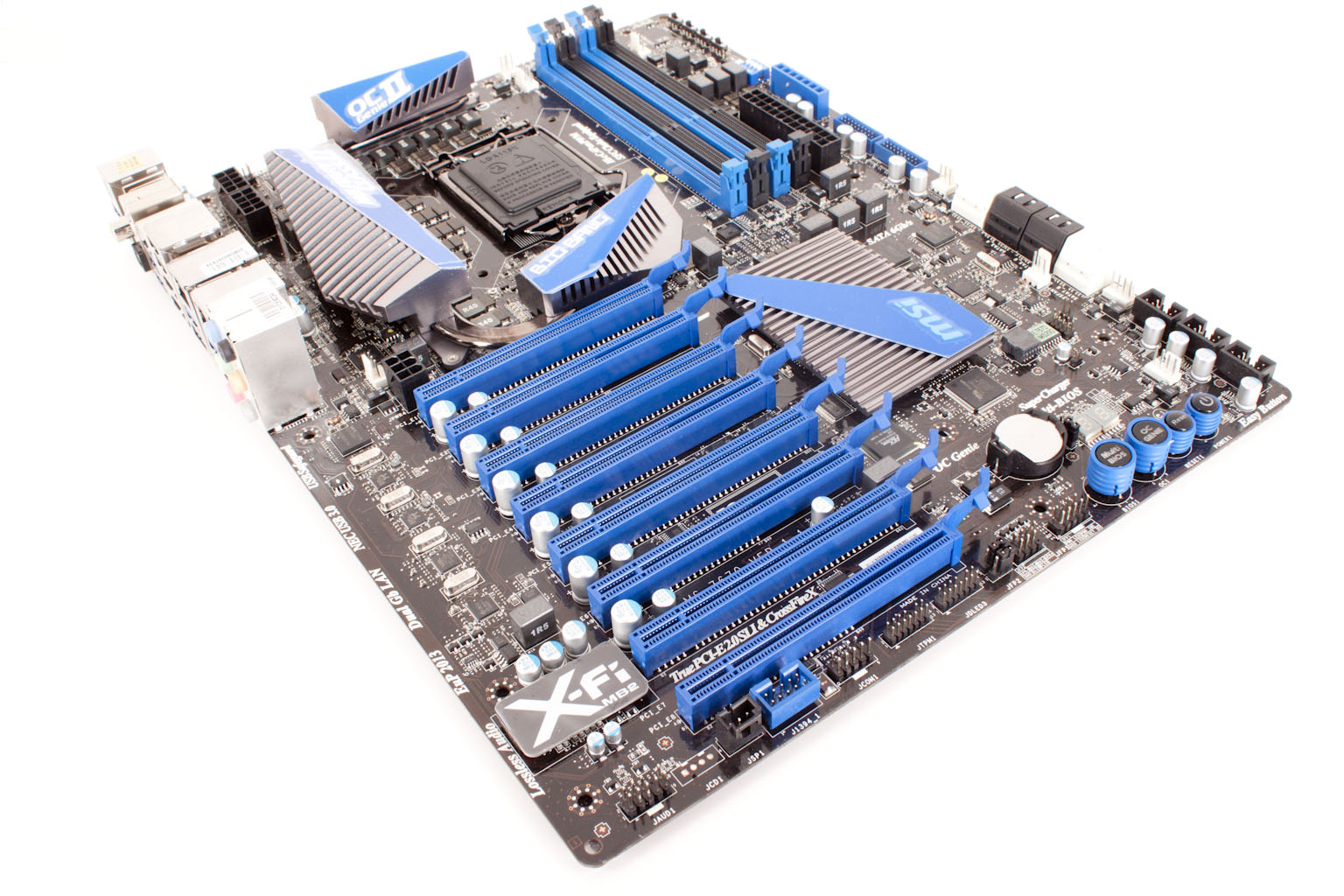
So where should we start? How about right up at the top where the RAM is at? Ok looking up here we find a few interesting items scattered amongst the normal stuff. There are two USB 3.0 headers here plus a voltage mount block. This block is nice in that it helps to keep your probe in contact without having it slide over the board. We also find a dipswitch block on the board right next to this. This block handles overvolting certain components; switch one is listed as reserved while the other three handle the CPU I/O, DRAM and SA in that order. Setting this to “on” gives a 200mV boost to these components while also increasing the max voltage range in the BIOS. The next unusual item is another bank of switches; these are there to enable or disable one of the four PCIe x16 slots on the board. Scattered around the board are a series of jumpers and mini rheostats (dials) that will let you control different voltages on the board with the use of a jewelers screw driver. By default they are disabled. To enable them you have to close the jumper that is near them.
 |
 |
 |
Moving on to the CPU side of things we find more of the new design choices that MSI has made. We find a large number of the Hi-c CAPS that we talked about right next to a bank coils of that are usually found on video cards and not motherboards. Behind these (under the heatsink) are the “server” class MOSFETs that we talked about a little earlier. These are (in theory) able to perform significantly faster than a typical MOSFET (around four times faster). This makes them significantly more efficient (which also can mean cooler running). With all of these features and high-performance parts MSI must be planning on needing a lot of power. They have thrown in two 8-pin Aux power connectors to keep the 12V power flowing. They have also widened the heat pipe that runs between the heatsinks. Moving down to the lower half of the board we find a whole lot of slots! Good grief MSI stacked them in here. Ok to get down to things; there are two slots that are x16 mechanical and electrical (slots one and five). These are actually tied to two other slots making them a bank. Slot one is tied to slot 3 while slot five is tied to slot seven. When you have a card in any of these slots then the other will drop back to x8 electrical. The other slots (2, 4, 6 and 8) are pinned for x8 electrical but they will not run at that speed. You only get x1 lanes on these slots. To get all these extra lanes MSI dropped a Lucid LT22102 chip onto the board. This chip provides an extra 32 lanes of bandwidth and provides the Lucid Hydralogix Multi-GPU technology for the Big Bang Marshal. So while the MSI Big Bang Marshal looks impressive with all those x16 slots; it really only has four available for use with GPUs, the others are kinds of for show. To make sure there is enough power to run all of this MSI put in a 6-Pin PCIe header for power. This single port can provide almost as much power as two Molex connectors.

In this next shot there is a lot going on that we need to talk about. We already told you about the LT22102 chip that is being used for GPU bandwidth and now we are going to tell you about another bridge on here to help out with the PCIe lane challenged Sandy Bridge and P67. This Is a PLX bridge and is here to add the needed lanes for the three NEC USB3.0 controllers that are here. It also handles the Marvell SE9128 controller (for SATA 3.0). Without this you would not have enough bandwidth to run everything and the Big Bang would be a dud. MSI also put their onboard controls here. There are the usual; power and reset but there is also the OCGenie and the Multi BIOS switch here as well.
 Flipping over to the I/O ports we find a staggering number of USB 3.0 ports on the back. Now I know we just told you that there are only 3 NEC controllers on the board and there are. The eight that are here are courtesy of a little port replicator hidden right behind the dual LAN ports. This is a VIA VL810 hub chip and it takes the single NEC controller that is up by the PCIe 1 port and splits the two normal ports into eight. The dual LAN ports here are run by a pair of Realtek RTL8111E chips.