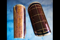
IBM scientists say that since these circuits are so thin, they can be stacked on each other in large numbers and thus provide vastly improved performance. On one slip fits 10 billion transistors, and to operate they require voltage of only 0.6 volts, which makes them extremely frugal and energy efficient.
IBM highlighted how the technology that was used to "peel" the semiconductor layers so thin from a piece of silicon can be used for other applications, such as making smaller and more environmentally friendly lights.
[Ed – when this news first hit many wondered what this would be used for. There are many applications for this including medical implants that fit into the body better and without being as intrusive. Another larger part of this technology is wearable computing which many companies have been working towards for a long time. ]
What do you think about IBM’s new technology? Tell us in our Forum


