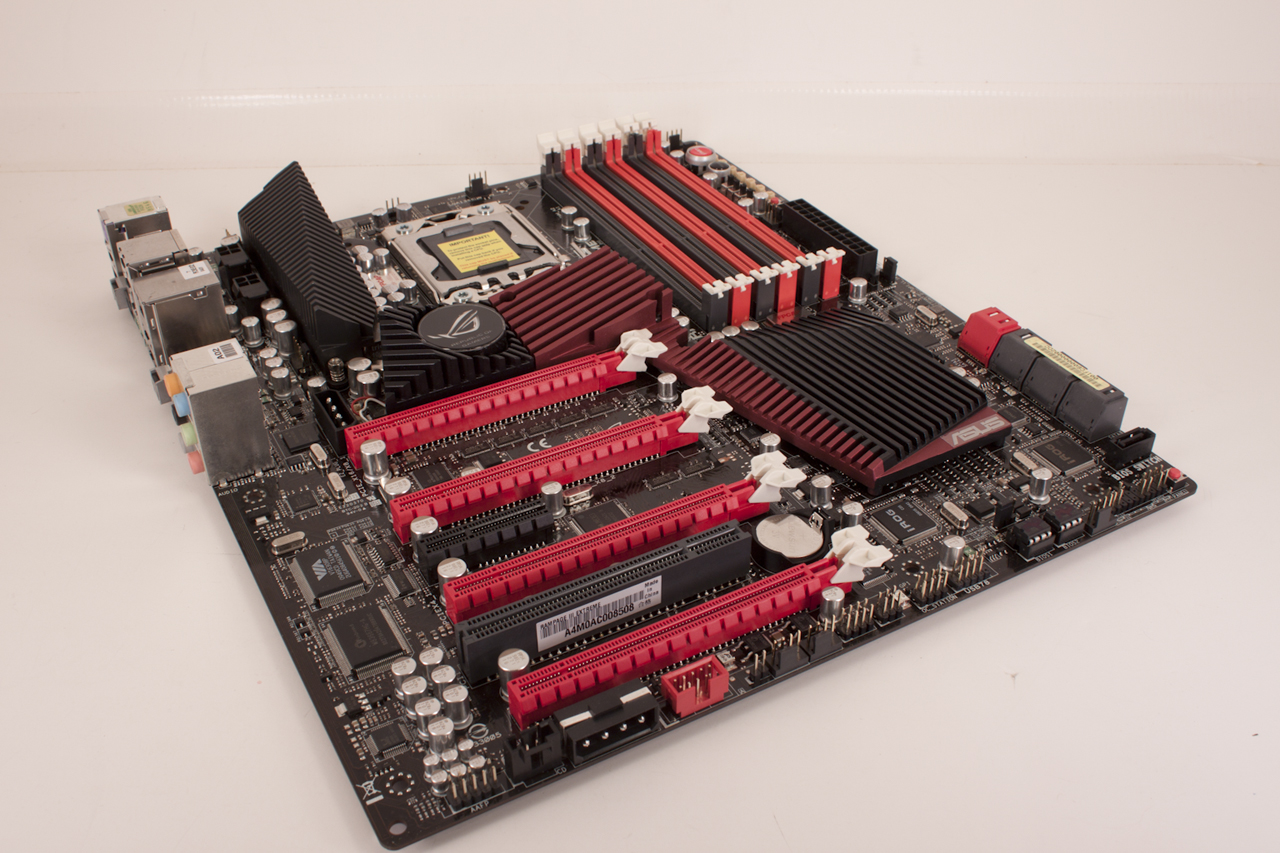
The Layout -
The layout of any motherboard is important. Even simple mistakes in component placement or the signal traces can cause major issued in performance and stability. With the ATX form factor we find that this is even truer; the devices we drop onto them demand more and cleaner power while the signal speeds pus faster and faster.
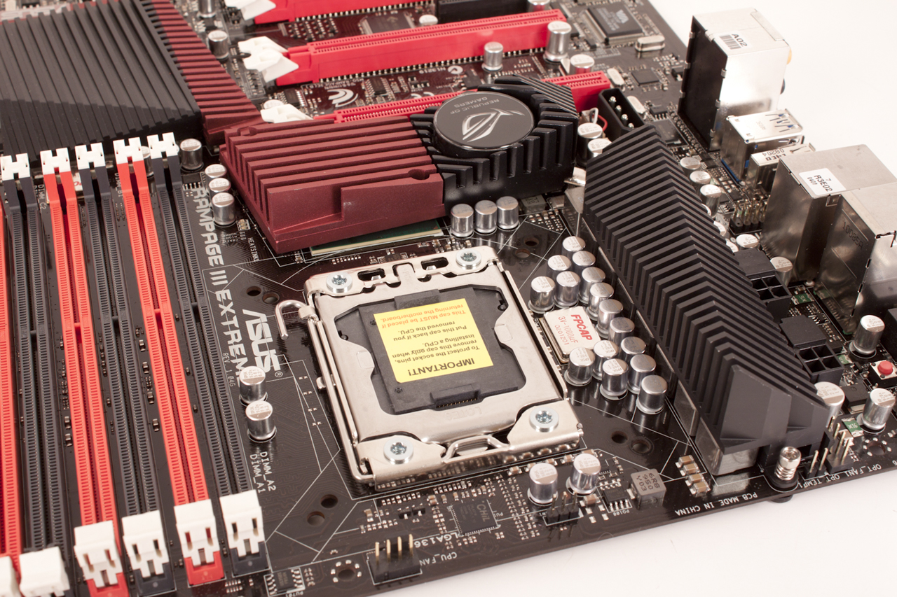
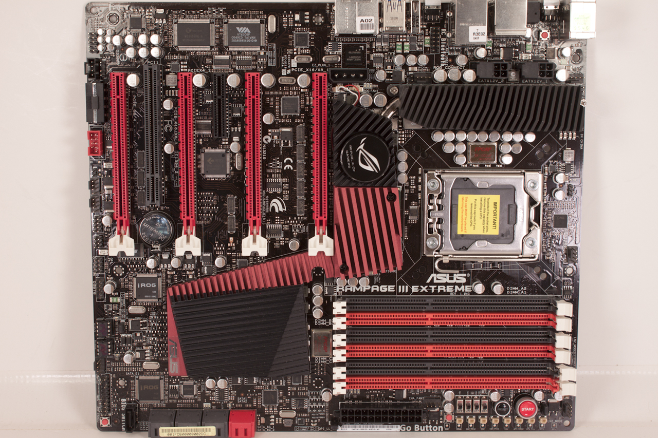 When we look at the4 top down view we can already ID a couple of small issues. The first and most glaring one is the proximity of the primary PCIe slot to the NB and NF 200 cooling group. It is almost right on top of it! To make matters a little more complicated we find that the PCIe release tab is also right over the heatpipe extension that connects the NB to the Southbridge cooling.
Now we mentioned that there were a couple of items that jumped out. The second is also related to the top PCIe slot. When using a longer add-in GPU like the AMD 58xx and upper end nVidia GTX 2xx and 4xx cards they crowd the RAM slots. Now Asus has begun using a one-armed system to prevent the RAM being locked in, but there is a smaller issue here. You cannot use any of the Air coolers for RAM. Neither our Kingston, nor the Corsair we have would work at all. It is small issue but one that could mean a few extra MHz on the RAM end of things when you are going for extreme clocks and high 3D Marks scores.
 |
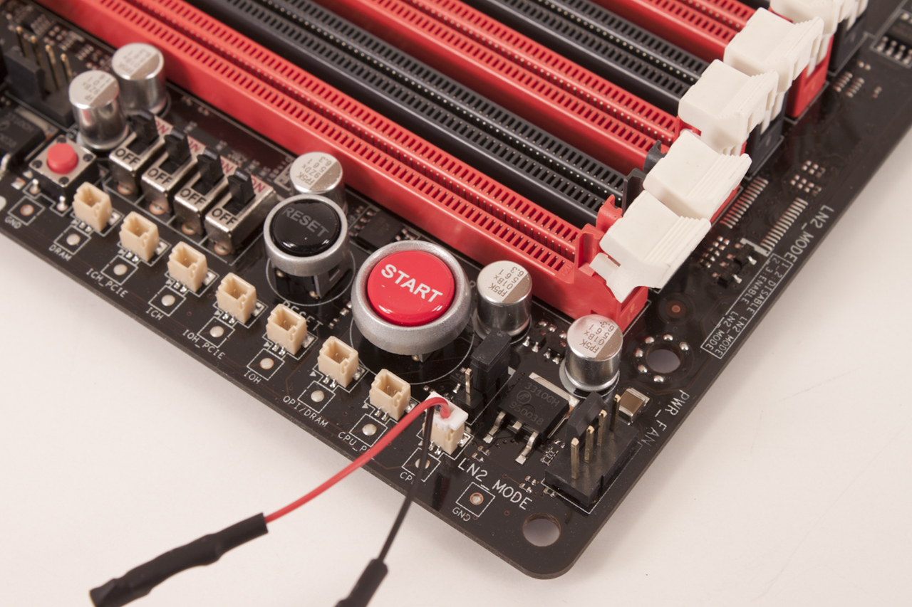 |
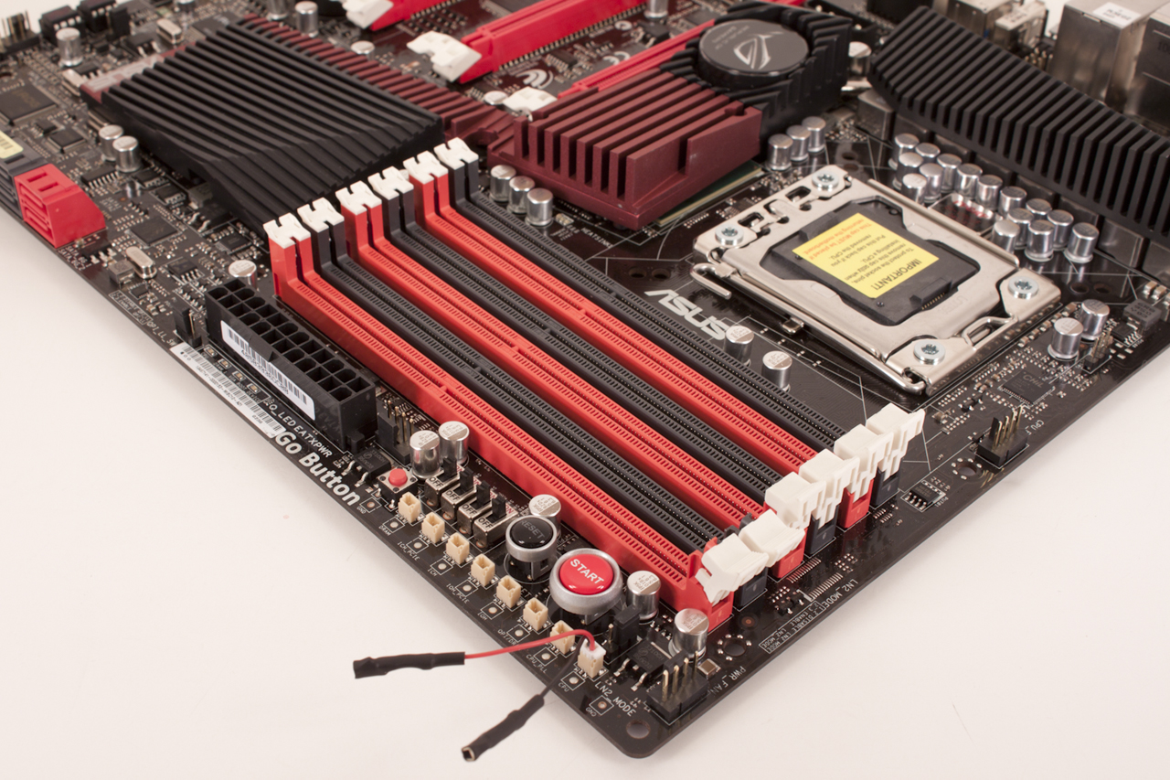
Moving on from the issues we noted, the rest of the board is laid out very well for both the bench top overclocker and the enthusiast that plans on shoving this into a high-end case. Going back to the RAM slots we find the first group of bench features. As you can clearly see in these images Asus has moved the power and reset switches to the top of the board. In this position they are very accessible. Right in front of them is a row of voltage monitoring points. Here you have a nice option. You can either use the solder pad or, you can use the included (only one) cable adapter to monitor one voltage point continuously.
You will also note a bank of four switches. These give you the ability to manually disable the PCIe slots. Removing these from the mix (when not in use) can greatly improve your stability at high BCLKs. We also get a glimpse of the Go Button. This is a multi-purpose button that not only acts as a MemOK! Button during post but can also quickly switch to a customizable overclock setting that you can store through the BIOS. At the top of the group here is an LN2 mode jumper, another item for the crazy overclocker that is using super cooling to achieve massive speeds.
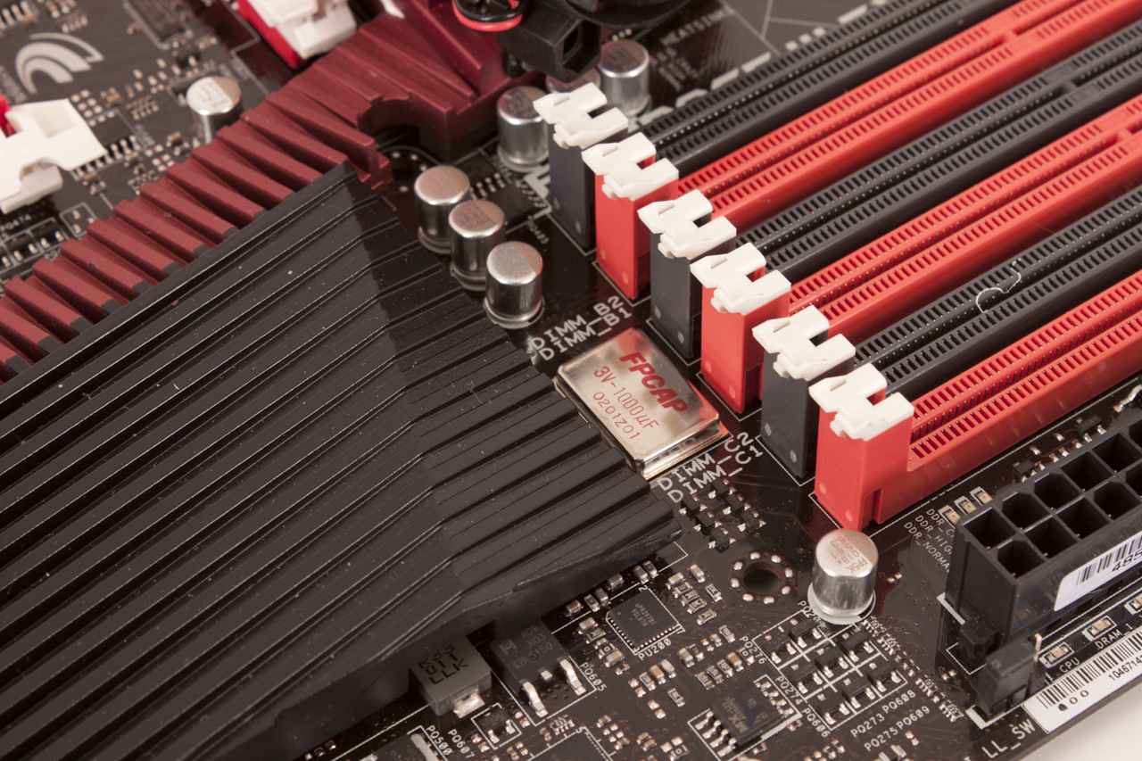
Looking at the CPU space we do find a rather clean layout with the exception that we noted above. The NB and NF200 are a little close to the CPU socket. However, this was probably a design trade-off in order to have room for good cooling and the four PCIe x16 mechanical slots on the board. Looking at this picture you will see the large flat FPCAP. This is a nice touch as it is a much higher-end component than the others around it. It allows much cleaner and stable power to flow to the CPU. This particular one also has a significantly higher voltage tolerance allowing you to maintain clean power at higher voltages. Asus has included another one right next to the RAM slots to ensure good, stable power to both of these critical components.
 |
 |
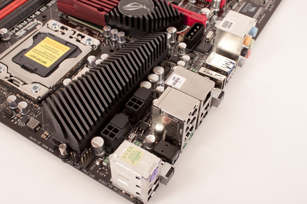
Behind the VRM cooling heatsink are two 8-pin aux ATX power ports. As we have mentioned before the current crop of components require more and cleaner power even at stock speeds. If you really want to push things you have an even greater need of this type of power. Asus has you covered here. You not only have these two 8-pin connectors, but two additional 4-pin Molex connectors. One is right next to the NF200 cooler and the other is along the bottom edge of the board. Also taking a peak out at us in this shot is the LN2 reset button. You can just see it reflected in on the side of the USB/e-SATA stack. The LN2 reset button allows you to reset the power to the board in the event that it does not power up at subzero temperatures. Think of this as a jump start. The button quickly interrupts power and then allows it to flow back at full force to the board.
 |
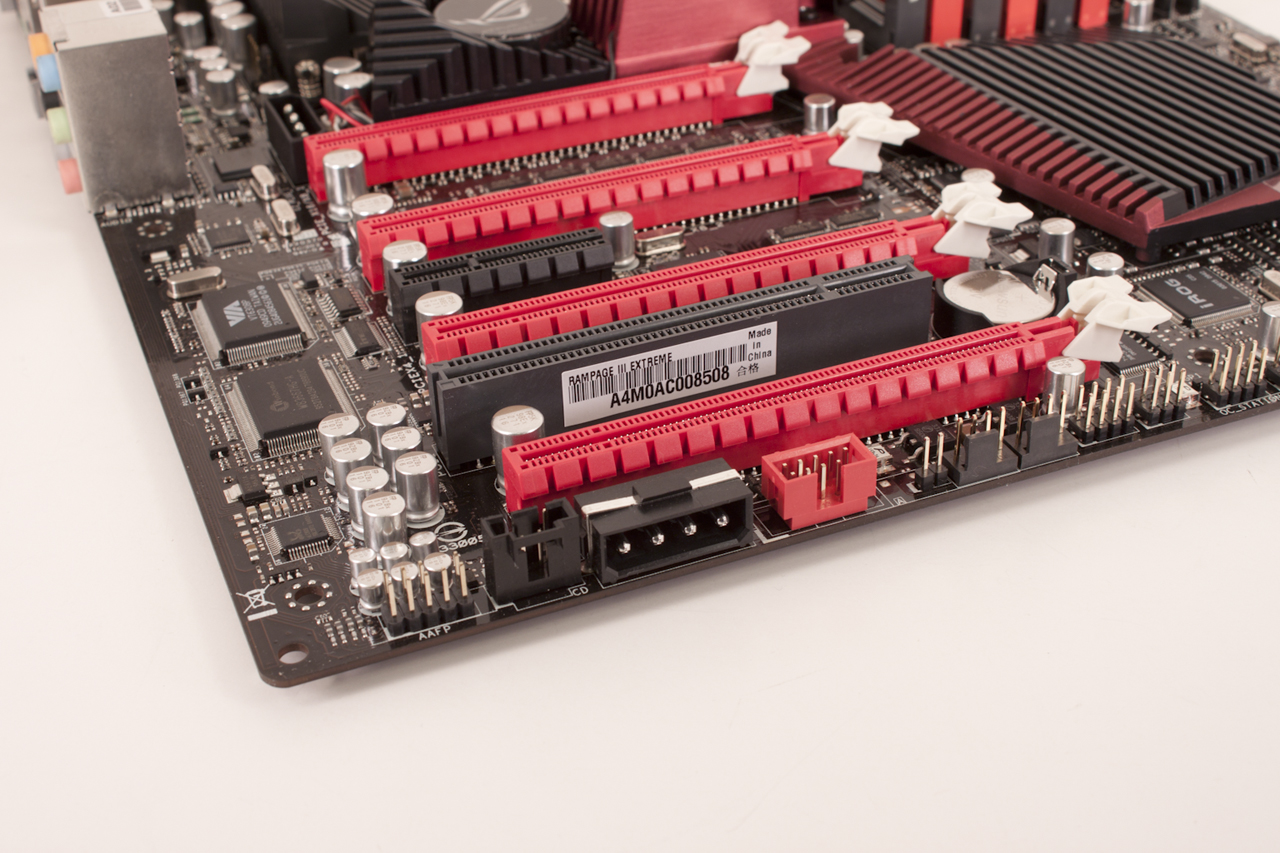 |
In the next shot we see the reason for the cramped CPU space. The four PCIe x16 mechanical slots; now not all of these are going to give you a full 16 PCIe 2.0 lanes. The reason this is an important thing to note is the bandwidth available. A single PCIe Gen 2 lane has a theoretical bandwidth of 500MB/s with 16 lanes that is 8000MB/s or around 8GB/s. It then follows that at x8 or x4 you get considerable reduction in bandwidth. The four slots have to share 32 lanes from the NF200. So no matter the configuration you are not getting more than 16BG/s of bandwidth. If you are looking for dual GPU SLI or Crossfire at x16 then slots 1 and 3 are the ones you will want to use as they are both capable of x16. Tri SLI is slots 1, 2, and 3 with gets you x16 on slot one and x8 on slots 2 and 3. Quad Crossfire drops all the slots to x8. As you can see, doing this reduces the band width to the extra GPUs (over two) and can also reduce the benefit from adding them. Asus does offer an add-on board to correct this, but as we do not have one, we cannot comment on its use or performance.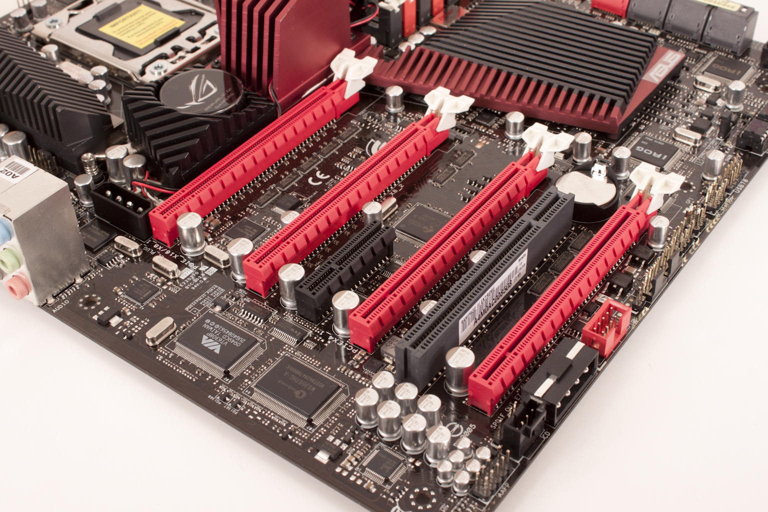
Looking at the other side of the board we get a good look at the SATA ports. As is typical on the Intel boards there are 6 SATA 2.0 ports and two SATA 3.0 ports. The SATA 3.0 ports are controlled by a Marvell controller (again as usual). You can also see the connectors for a set of USB ports, and on the very left edge of the image you can just make out the OC Station connector. This is another component that we do not have (yet). You can also see the dual BIOS chips; this is an excellent feature for overclockers and enthusiasts alike. It gives you a backup of the current BIOS in case things go wrong and also allows you to maintain two different BIOS builds. This is great if you find that one BIOS works better for something (like BCLK overclocking) and you want to maintain it. You can bounce between these two BIOSes with the BIOS switch that is located in the corner.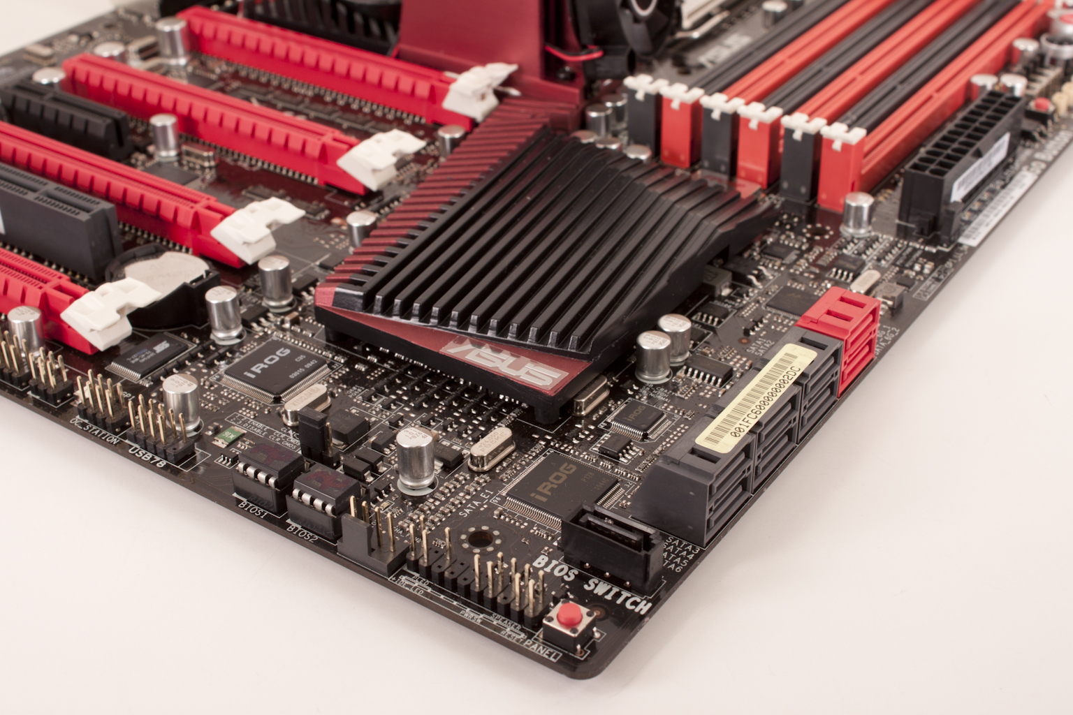
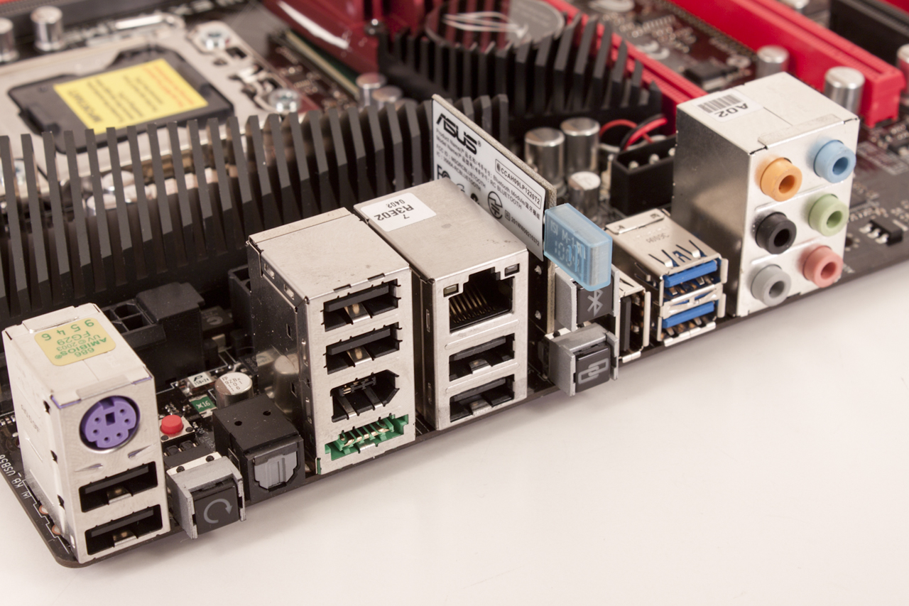 Whipping around to the back side of the board we find the ports. These are now pretty typical on an ATX board. You have a single PS/2 port multiple USB ports (there are 6 usable on the back of the RIIIE), e-SATA ports, a GBe LAN port, optical digital audio, and six 1/8th inch audio plugs. On the RIIIE we find a couple of extras. There is a vertical USB port that exists to run the ROG Connect feature, this is right next to the button that activates the feature. On top of that is the Bluetooth module (a feature rarely found on desktop motherboards) with its own on/off button. The CMOS reset button is familiar to anyone that has owned a top end motherboard (at least now it is). The firewire port is simply a nice extra touch.
Overall, the RIIIE is a well laid out board. There were some hard design choices that had to be made, but overall these were minor and were made with allowing the greatest advantage. As this is a board meant to be pushed (as you will see later) Asus has thrown in a few extras that we did not specifically cover in the layout. Some are feature specific so they will be talked about below.

